Following Professional Sd Card Pcb Layout Guidelines To Ensure High Speed Data Transfer And Signal Integrity - pcb layout: a comprehensive guide
If you are looking for High Speed Pcb Layout Guidelines - Design Talk you've came to the right place. We have 35 Pictures about High Speed Pcb Layout Guidelines - Design Talk like High Speed Pcb Layout Guidelines - Design Talk, PCB Layout Guidelines | Design Rules & Requirements | Tips and also High-Speed PCB Signal Integrity Design Tutorial - TechSparks. Here you go:
High Speed Pcb Layout Guidelines - Design Talk
 design.udlvirtual.edu.pe
High Speed Pcb Layout Guidelines - Design Talk
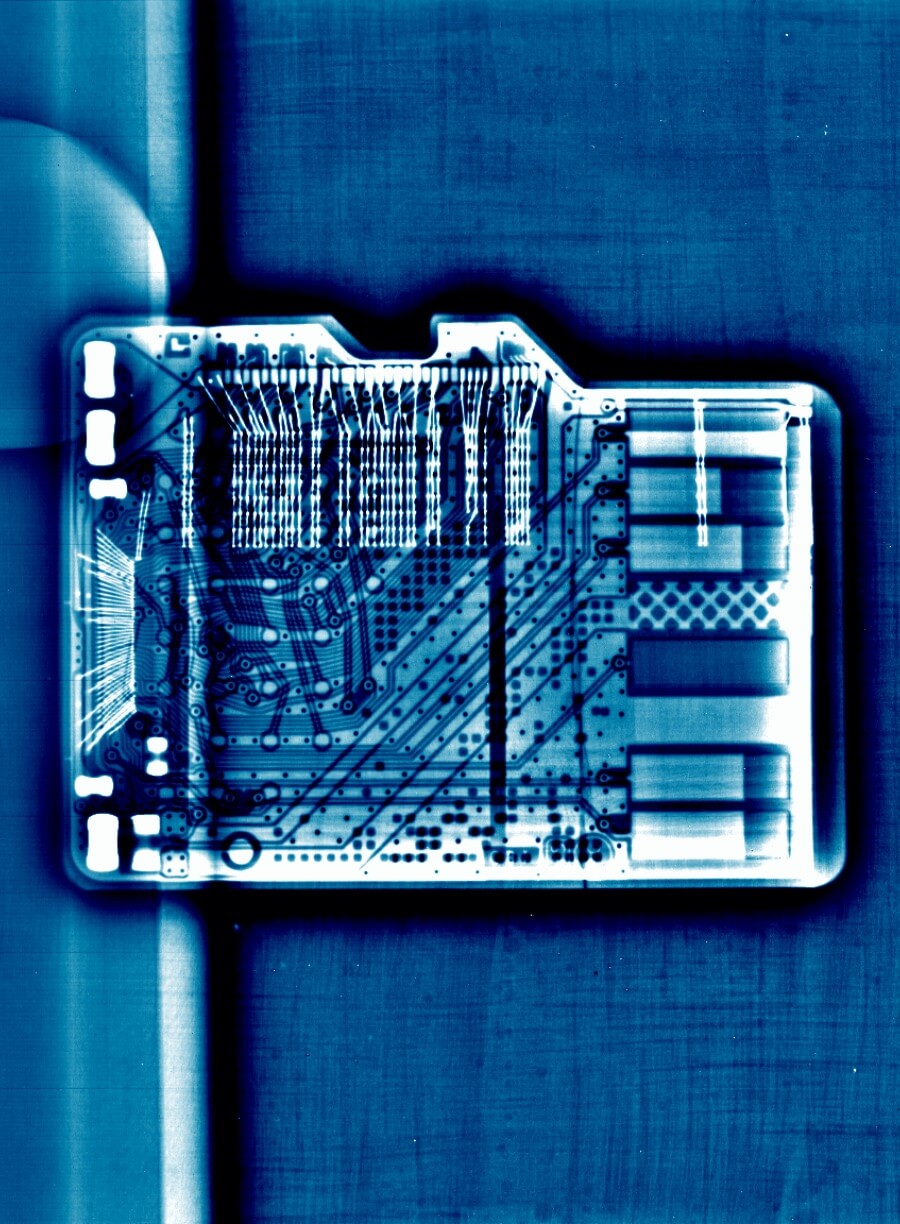
EMMC (micro)SD Card | KittenLabs
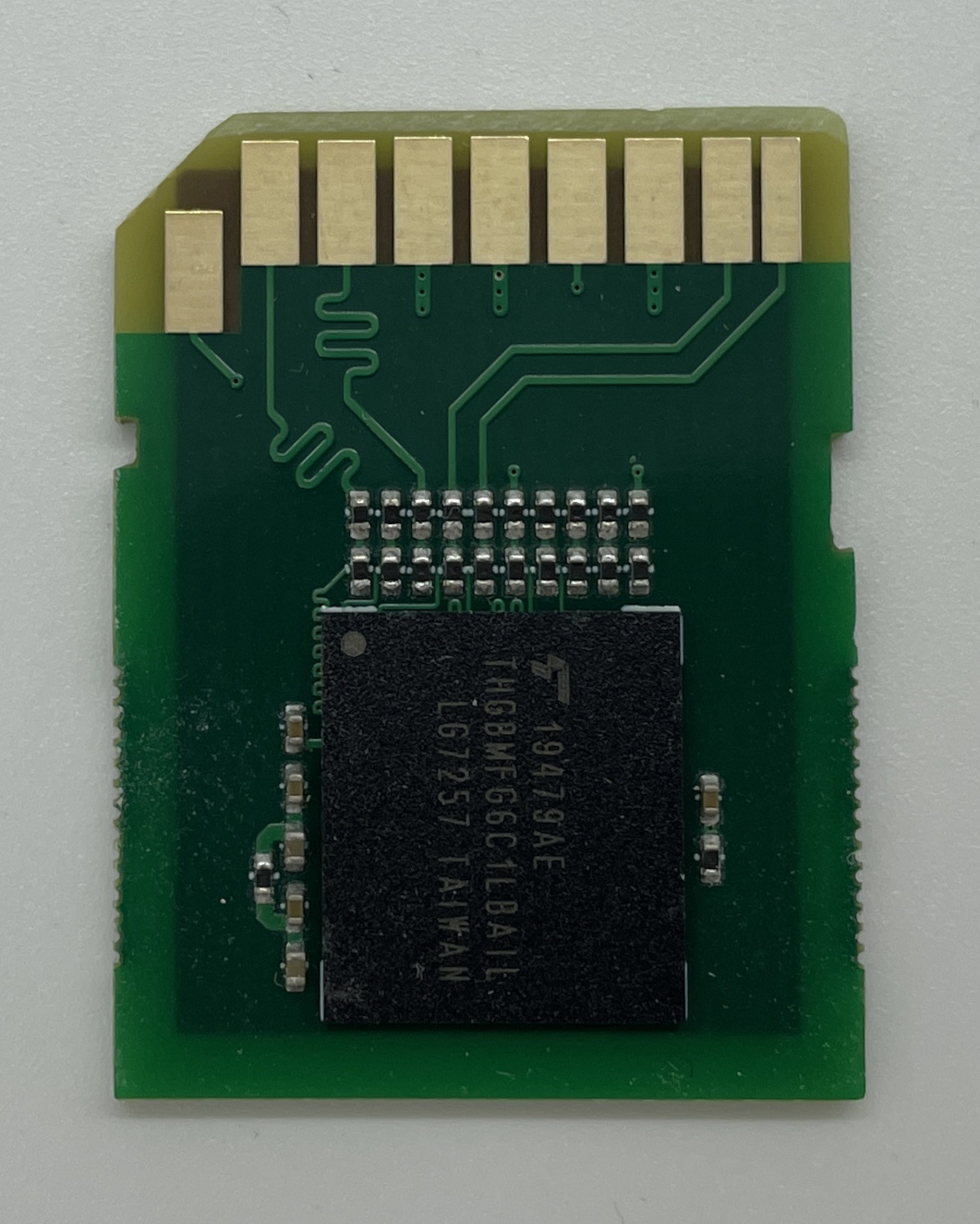 kittenlabs.de
eMMC (micro)SD card | KittenLabs
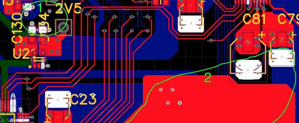
High Speed Signal Routing Guidelines At Brock Clemes Blog
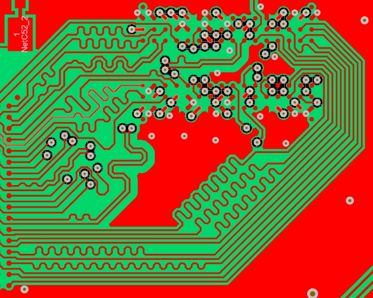 storage.googleapis.com
High Speed Signal Routing Guidelines at Brock Clemes blog
High Speed PCB Design: Routing, Impedance & Layout Techniques
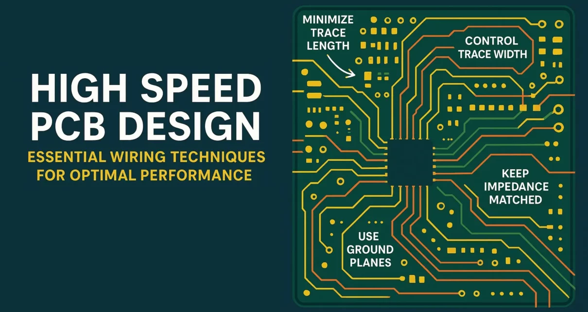 hackatronic.com
High Speed PCB Design: Routing, Impedance & Layout Techniques
PCB Layout Guidelines For High Speed Applications
 www.linkedin.com
PCB Layout Guidelines For High Speed Applications
Premium Photo | Digital Fiber Optic Cable With High Speed Data Transfer
 www.freepik.com
Premium Photo | Digital fiber optic cable with high speed data transfer ...
[Schematic And PCB Review Request] SD Card Reader + PowerBank : R
![[Schematic and PCB Review Request] SD Card reader + PowerBank : r](https://preview.redd.it/schematic-and-pcb-review-request-sd-card-reader-powerbank-v0-domvov12o6y91.png?width=2350&format=png&auto=webp&s=52d3a53cd0ceae2a9f73daf26fa7785dfa08de4a) www.reddit.com
www.reddit.com
[Schematic and PCB Review Request] SD Card reader + PowerBank : r ...
ESP32 - SD Card | ESP32 Tutorial
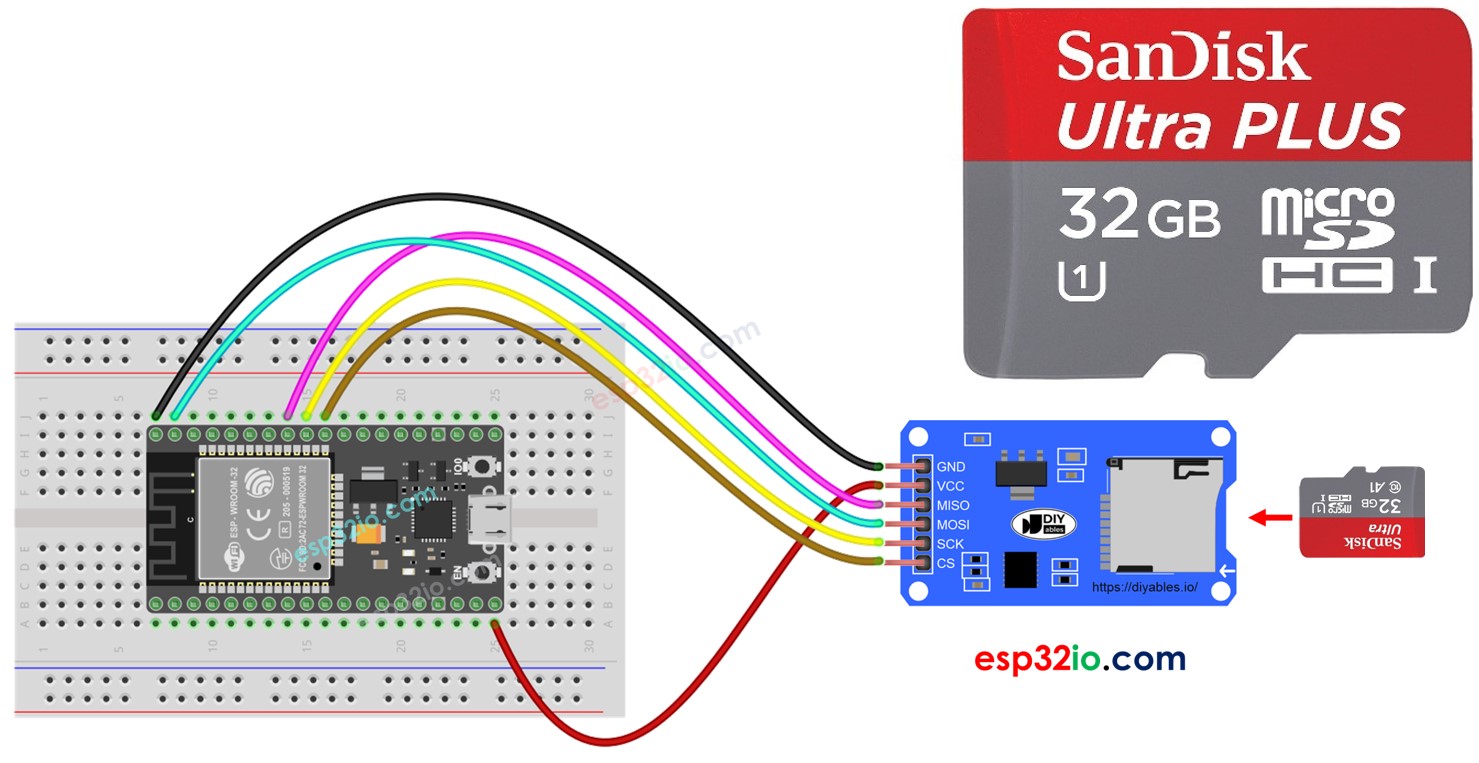 esp32io.com
ESP32 - SD Card | ESP32 Tutorial
GPU PCB: Structure, Function & Design Insights - GlobalWellPCBA
 www.globalwellpcba.com
GPU PCB: Structure, Function & Design Insights - GlobalWellPCBA
PCB Layers Explanation: Everything You Need To Know - TechSparks
 www.tech-sparks.com
PCB Layers Explanation: Everything You Need to Know - TechSparks
Signal Integrity Analysis | PCB Signal Integrity Solutions – GigHz
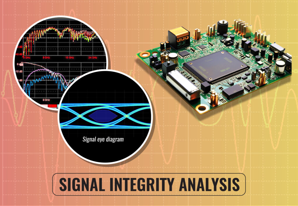 gighz.net
Signal Integrity Analysis | PCB Signal Integrity Solutions – GigHz
Professional SD Card Front And Back Vector Illustration Isolated On
 www.freepik.com
Professional SD Card Front and Back Vector Illustration Isolated on ...
Professional SD Card Front And Back Vector Illustration Isolated On
 www.freepik.com
Professional SD Card Front and Back Vector Illustration Isolated on ...
The Importance Of Signal Integrity In High-Speed PCB Design
 www.autodesk.com
The Importance of Signal Integrity in High-Speed PCB Design
Professional SD Card Front And Back Vector Illustration For Tech
 www.freepik.com
Professional SD Card Front and Back Vector Illustration for Tech ...
Fiber Optic High Speed Data Transfer Concept Stock Photo - Alamy
 www.alamy.com
Fiber optic high speed data transfer concept Stock Photo - Alamy
News
 www.e-kom.com
News
News
News
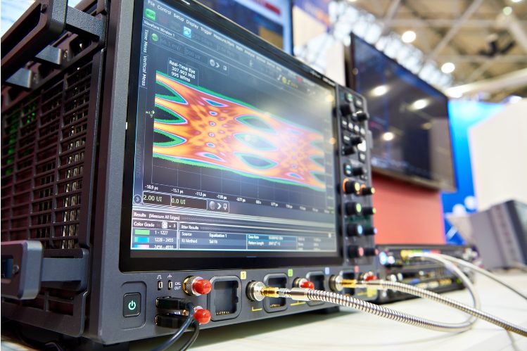
Signal And Power Integrity Fundamentals On High Speed - RayPCB
 www.raypcb.com
Signal and Power Integrity Fundamentals on High Speed - RayPCB
Professional SD Card Front And Back Vector Illustration Isolated On
 www.freepik.com
Professional SD Card Front and Back Vector Illustration Isolated on ...
Top 5 PCB Design Rules You Need To Know | PCB Design Blog | Altium
 resources.altium.com
Top 5 PCB Design Rules You Need to Know | PCB Design Blog | Altium
High-Speed PCB Signal Integrity Design Tutorial - TechSparks
 www.tech-sparks.com
High-Speed PCB Signal Integrity Design Tutorial - TechSparks
PCB Layout Guidelines | Design Rules & Requirements | Tips
 www.wellpcb.com
PCB Layout Guidelines | Design Rules & Requirements | Tips
Professional SD Card Data Recovery Services | DriveSavers Data Recovery
 drivesaversdatarecovery.com
Professional SD Card Data Recovery Services | DriveSavers Data Recovery
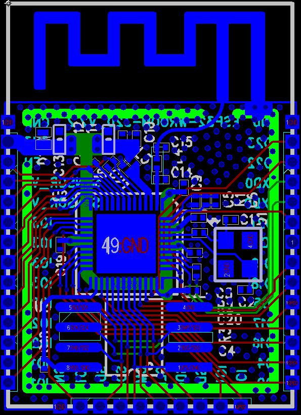
PCB Layout Design - ESP32 - — ESP Hardware Design Guidelines Latest
 docs.espressif.com
PCB Layout Design - ESP32 - — ESP Hardware Design Guidelines latest ...
Micro SD Card PCB Layout: Everything You Need To Know – Hillman Curtis
 hillmancurtis.com
Micro SD Card PCB Layout: Everything You Need to Know – Hillman Curtis ...
Redistribution Layer (RDL) Technology For ICs Package | Reversepcb
 reversepcb.com
Redistribution Layer (RDL) Technology for ICs Package | Reversepcb
Twisted Glowing Digital Cables In A Vibrant Pink And Purple Abstract
 www.dreamstime.com
Twisted Glowing Digital Cables in a Vibrant Pink and Purple Abstract ...
Micro SD Card PCB Layout: Everything You Need To Know – Hillman Curtis
 hillmancurtis.com
Micro SD Card PCB Layout: Everything You Need to Know – Hillman Curtis ...
PCB Layout Guidelines | Design Rules & Requirements | Tips
 www.wellpcb.com
PCB Layout Guidelines | Design Rules & Requirements | Tips
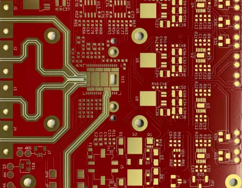
PCB Layout: A Comprehensive Guide - GlobalWellPCBA
 www.globalwellpcba.com
PCB Layout: A Comprehensive Guide - GlobalWellPCBA
PCB Design Layout Guidelines: Best Practices | EMA Design Automation
 www.ema-eda.com
PCB Design Layout Guidelines: Best Practices | EMA Design Automation
How To Read PCB Layout Design: Beginner’s Guide
 www.viasion.com
How to Read PCB Layout Design: Beginner’s Guide
Professional SD Card Data Recovery Services | DriveSavers Data Recovery
 drivesaversdatarecovery.com
Professional SD Card Data Recovery Services | DriveSavers Data Recovery
Getting Started With RF PCB Layout Guidelines
 www.hemeixinpcb.com
Getting Started With RF PCB Layout Guidelines
Pcb layout guidelines. Premium photo. high speed pcb layout guidelines